|
|
|
|
|
|
|
|
|
|
|
|
|
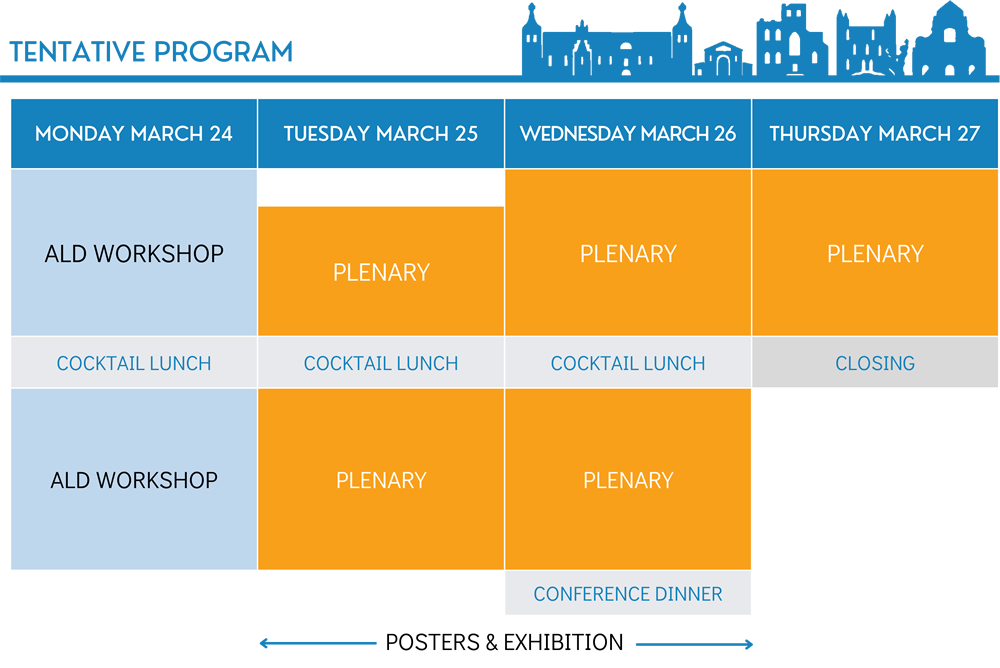
Tue 25 |
|
Wed 26 |
|
Thu 27 |
|
|
|
|
|
|
|
|
|
|
|
|
|
|
|
|
|
|
|
|
|
|
|
|
|
|
|
|
|
|
|
|
|
|
|
|
|
|
|
|
|
|
|
|
|
|
|
|
|
|
|
|
|
|
|
09:00-09:15 |
|
Opening - Christopher J. Wilson |
|
|
|
|
|
|
|
|
|
|
|
|
|
|
|
|
Chairperson: Christopher Wilson & Paulina Rincon |
|
|
|
|
|
|
|
|
|
|
|
|
|
|
|
09:15-09:55 |
|
INVITED |
|
The Metallization Routing to Two Trillion Dollars |
|
Anand Murthy,
Lam, USA |
|
 |
|
|
|
|
|
|
|
|
|
|
|
|
|
|
|
|
09:55-10:35 |
|
INVITED |
|
From stamp to wafer - How complex ALD processes become exponentially harder to control on fab-friendly scale |
|
Henrik H. Sønsteby,
University of Oslo, Norway |
|
|
|
|
|
|
|
|
|
|
|
|
|
|
|
|
|
|
|
|
|
|
|
|
|
|
|
|
|
|
|
|
Chairperson: Magali Gregoire & Fabrice Nemouchi |
|
|
|
|
|
|
|
|
|
|
|
|
|
|
|
11:05-11:45 |
|
INVITED |
|
Selective and Self-Limited Process Technologies to Enable Ångstrom Scale Integrated Circuits |
|
Robert Clark,
TEL, USA |
|
|
|
|
|
|
|
|
|
|
|
|
|
|
|
|
|
|
11:45-12:25 |
|
INVITED |
|
ALD and AS-ALD of Metallic Films with New Precursors and Approaches |
|
Mikko Ritala,
University of Helsinki, Finland |
|
|
|
|
|
|
|
|
|
|
|
|
|
|
|
|
|
|
|
|
|
|
|
|
|
|
|
|
|
|
|
|
Chairperson: Stefan Schulz & Jan Willem Maes |
|
|
|
|
|
|
|
|
|
|
|
|
|
|
|
13:25-14:05 |
|
INVITED |
|
Time for ALD Metals: Enabling the next generation of leading-edge devices |
|
Chiyu Zhu,
ASM, Finland |
|
|
|
|
|
|
|
|
|
|
|
|
|
|
|
|
|
|
14:05-14:45 |
|
INVITED |
|
In situ study of the synthesis of lamellar metal chalcogenides by alternating deposition of organic & inorganic molecules |
|
Hubert Renevier,
Grenoble INP-PhElMa UGA , France |
|
|
|
|
|
|
|
|
|
|
|
|
|
|
|
|
|
|
|
|
|
|
|
|
|
|
|
|
|
|
|
|
Chairperson: Christophe Detavernier & Claudia Wiemer |
|
|
|
|
|
|
|
|
|
|
|
|
|
|
|
15:15-15:55 |
|
INVITED |
|
Understanding and predicting interconnect metal deposition and morphology from atomic scale simulations |
|
Cara-Lena Nies,
Tyndall National Institute, Ireland |
|
|
|
|
|
|
|
|
|
|
|
|
|
|
|
|
|
|
15:55-16:35 |
|
INVITED |
|
Next Generation Microelectronics Devices Enabled by Atomic Layer Deposition |
|
Mark Saly,
Applied Materials, USA |
|
|
|
|
|
|
|
|
|
|
|
|
|
|
|
|
|
|
16:35-17:35 |
|
Panel discussion |
|
|
|
|
|
|
|
|
|
|
|
|
|
|
|
. |
|
|
|
|
|
|
|
|
|
|
|
|